VOXLS 30 C 320
320 kV Microfocus Reflection Target Penta Source Functionality available Flat Panel Detector Max Scan Volume: 610mm (Ø) × 1050mm (H) Max Sample Mass: 100kg central load System Mass: 10,350kg
Nikon’s XT V range comprises world-class X-ray and CT systems for non-destructive inspection of electronic components (PCBs, BGAs, chips and much more).
With sub-micron feature recognition, the XT V system range meets today’s need for high performance, non-destructive inspection of complex electronic components. Nikon’s Xi Nanotech X-ray source paired with industry leading flat panel detectors produces best-in-class image quality, with seamless transition between 2D and 3D inspection.
updated: May 8, 2023
Superior X-Ray Source
Nikon’s market-leading Xi Nanotech X-ray microfocus source is unique due to its exclusive integral generator design and unparalleled 160kV maximum energy and 20W true-target power.
PCB Analysis Suite
PCB Analysis Suite is capable of advanced measurement and analysis of BGA, bond wires, PTH and complex packages such as PoP on multi-layered boards, with automated pass/fail inspection and reporting.
Oblique Angle Concentric Imaging
Extreme oblique angle field of view up to 90°, with 360° sample rotation, maintains the region of interest thanks to intelligent software and hardware.
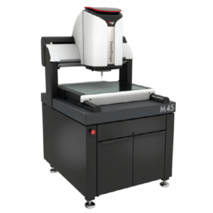
SmartScope M45
quick view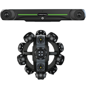
NimbleTrack Wireless 3D Scanning System
quick view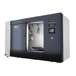
VOXLS 30 C 320
quick view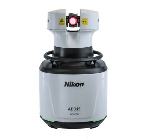
APDIS Laser Radar
quick view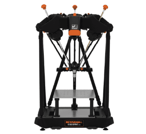
Equator 300 EH
quick view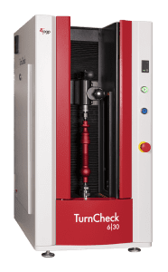
TurnCheck Series-6
quick view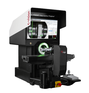
C-vision Benchtop Video Contour Projector
quick view
MiSTAR 555
quick view